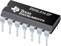
SN54LS14-SP 六路施密特触发反向器

Each circuit functions as an inverter, but because of the Schmitt action, it has different input threshold levels for positive-going (VT+) and negative-going (VT–) signals.
These circuits are temperature compensated and can be triggered from the slowest of input ramps and still give clean, jitter-free output signals
|
SN54LS14-SP |
| Voltage Nodes (V) |
5 |
| No. of Gates |
6 |
| Vcc range (V) |
4.5 to 5.5 |
| Input Level |
TTL |
| Output Level |
TTL |
| Technology Family |
LS |
| Rating |
Space |
| Pin/Package |
14CDIP, 14CFP |
SN54LS14-SP 特性
- Operation From Very Slow Edges
- Improved Line-Receiving Characteristics
- High Noise Immunity
SN54LS14-SP 芯片订购指南
| 器件 |
状态 |
温度 |
价格(美元) |
封装 | 引脚 |
封装数量 | 封装载体 |
丝印标记 |
| 5962-9665801VCA |
ACTIVE |
-55 to 125 |
81.30 | 100u |
CDIP (J) | 14 |
1 | TUBE |
|
| 5962-9665801VDA |
ACTIVE |
-55 to 125 |
122.40 | 100u |
CFP (W) | 14 |
1 | TUBE |
|
SN54LS14-SP 应用手册
SN54LS14-SP 质量与无铅数据
| 器件 |
环保计划* |
铅/焊球涂层 |
MSL 等级/回流焊峰 |
环保信息与无铅 (Pb-free) |
DPPM / MTBF / FIT 率 |
| 5962-9665801VCA |
TBD |
A42 |
N/A for Pkg Type |
5962-9665801VCA |
5962-9665801VCA |
| 5962-9665801VDA |
TBD |
A42 |
N/A for Pkg Type |
5962-9665801VDA |
5962-9665801VDA |
SN54LS14-SP 应用技术支持与电子电路设计开发资源下载
- SN54LS14-SP 数据资料 dataSheet 下载.PDF
- TI 德州仪器缓冲器、驱动器/收发器产品选型与价格 . xls
- (选择指南)逻辑器件指南 2009 (Rev. Z)
- (用户指南)LOGIC Pocket Data Book
- (用户指南)Signal Switch Data Book
- Logic Cross-Reference (PDF 2938 KB)

