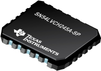
SN54LVCH245A-SP 具有三态输出的八路总线收发器

The SN54LVCH245A octal bus transceiver is designed for 2.7-V to 3.6-V VCC operation, and the SN74LVCH245A octal bus transceiver is designed for 1.65-V to 3.6-V VCC operation.
Inputs can be driven from either 3.3-V or 5-V devices. This feature allows the use of these devices as translators in a mixed 3.3-V/5-V system environment.
These devices are fully specified for partial-power-down applications using Ioff. The Ioff circuitry disables the outputs, preventing damaging current backflow through the devices when they are powered down.
To ensure the high-impedance state during power up or power down, OE\ should be tied to VCC through a pullup resistor; the minimum value of the resistor is determined by the current-sinking capability of the driver
| SN54LVCH245A-SP | |
| Voltage Nodes (V) | 3.3, 2.7, 2.5, 1.8 |
| Vcc range (V) | 2.0 to 3.6 |
| Input Level | TTL/CMOS |
| Output Level | LVTTL |
| Output Drive (mA) | -24/24 |
| No. of Outputs | 8 |
| No. of Bits | 8 |
| Logic | True |
| Static Current | 0.01 |
| tpd max (ns) | 7 |
| Rating | Space |
| Technology Family | LVC |
SN54LVCH245A-SP 特性
- Operate From 1.65 V to 3.6 V
- Inputs Accept Voltages to 5.5 V
- Max tpd of 6.3 ns at 3.3 V
- Typical VOLP (Output Ground Bounce) <0.8 V at VCC = 3.3 V, TA = 25°C
- Typical VOHV (Output VOH Undershoot) >2 V at VCC = 3.3 V, TA = 25°C
- Support Mixed-Mode Signal Operation on All Ports (5-V Input/Output Voltage With 3.3-V VCC)
- Ioff Supports Partial-Power-Down Mode Operation
- Bus Hold on Data Inputs Eliminates the Need for External Pullup/Pulldown Resistors
- Latch-Up Performance Exceeds 250 mA Per JESD 17
- ESD Protection Exceeds JESD 22
- 2000-V Human-Body Model (A114-A)
- 200-V Machine Model (A115-A)
SN54LVCH245A-SP 芯片订购指南
| 器件 | 状态 | 温度 | 价格(美元) | 封装 | 引脚 | 封装数量 | 封装载体 | 丝印标记 |
| 5962-9754301V2A | ACTIVE | -55 to 125 | 142.95 | 100u | LCCC (FK) | 20 | 1 | TUBE | |
| 5962-9754301VRA | ACTIVE | -55 to 125 | 138.00 | 100u | CDIP (J) | 20 | 1 | TUBE | |
| 5962-9754301VSA | ACTIVE | -55 to 125 | 138.00 | 100u | CFP (W) | 20 | 1 | TUBE |
SN54LVCH245A-SP 应用手册
SN54LVCH245A-SP 质量与无铅数据
| 器件 | 环保计划* | 铅/焊球涂层 | MSL 等级/回流焊峰 | 环保信息与无铅 (Pb-free) | DPPM / MTBF / FIT 率 |
| 5962-9754301V2A | TBD | POST-PLATE | N/A for Pkg Type | 5962-9754301V2A | 5962-9754301V2A |
| 5962-9754301VRA | TBD | A42 | N/A for Pkg Type | 5962-9754301VRA | 5962-9754301VRA |
| 5962-9754301VSA | TBD | Call TI | N/A for Pkg Type | 5962-9754301VSA | 5962-9754301VSA |
SN54LVCH245A-SP 应用技术支持与电子电路设计开发资源下载
- SN54LVCH245A-SP 数据资料 dataSheet 下载.PDF
- TI 德州仪器触发器/锁存器/寄存器产品选型与价格 . xls
- (用户指南)LOGIC Pocket Data Book
- (用户指南)Signal Switch Data Book
- (用户指南)LVC and LV Low-Voltage CMOS Logic Data Book
- (选择指南)逻辑器件指南 2009 (Rev. Z)
- (选择指南)小尺寸逻辑器件指南 (Rev. D)
- 2008年第一季度通信基础设施方案指南 (Rev. G)
- Communications Infrastructure Solutions Guide 1Q2010
- Design Summary for WCSP Little Logic
- Standard Linear & Logic for PCs, Servers & Motherboards
- STANDARD LINEAR AND LOGIC FOR DVD/VCD PLAYERS
- Military Low Voltage Solutions
- Low-Voltage Logic (LVC) Designer's Guide
- Logic Cross-Reference
