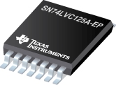
SN74LVC125A-EP 具有三态输出的增强型产品四路总线缓冲器闸

This quadruple bus buffer gate is designed for 1.65-V to 3.6-V VCC operation.
The SN74LVC125A features independent line drivers with 3-state outputs. Each output is disabled when the associated output-enable (OE) input is high.
To ensure the high-impedance state during power up or power down, OE should be tied to VCC through a pullup resistor; the minimum value of the resistor is determined by the current-sinking capability of the driver.
Inputs can be driven from either 3.3-V or 5-V devices. This feature allows the use of this device as a translator in a mixed 3.3-V/5-V system environment
| SN74LVC125A-EP | |
| Voltage Nodes (V) | 3.3, 2.7, 2.5, 1.8 |
| Vcc range (V) | 1.65 to 3.6 |
| Logic | True |
| Input Level | TTL/CMOS |
| Output Level | LVTTL |
| Output Drive (mA) | -24/24 |
| No. of Outputs | 4 |
| tpd max (ns) | 4.8 |
| Static Current | 0.01 |
| Rating | HiRel Enhanced Product |
| Technology Family | LVC |
SN74LVC125A-EP 特性
- Controlled Baseline
- One Assembly/Test Site, One Fabrication Site
- Enhanced Diminishing Manufacturing Sources (DMS) Support
- Enhanced Product-Change Notification
- Qualification Pedigree(1)
- Operates From 1.65 V to 3.6 V
- Inputs Accept Voltages to 5.5 V
- Max tpd of 4.8 ns at 3.3 V
- Typical VOLP (Output Ground Bounce) <0.8 V at VCC = 3.3 V, TA = 25°C
- Typical VOHV (Output VOH Undershoot) >2 V at VCC = 3.3 V, TA = 25°C
- Latch-Up Performance Exceeds 250 mA Per JESD 17
- ESD Protection Exceeds JESD 22
- 2000-V Human-Body Model (A114-A)
- 200-V Machine Model (A115-A)
- 1000-V Charged-Device Model (C101)
SN74LVC125A-EP 芯片订购指南
| 器件 | 状态 | 温度 | 价格(美元) | 封装 | 引脚 | 封装数量 | 封装载体 | 丝印标记 |
| SN74LVC125AIPWREP | ACTIVE | -40 to 85 | 0.20 | 1ku | TSSOP (PW) | 14 | 2000 | LARGE T&R | |
| SN74LVC125AMDREP | ACTIVE | -55 to 125 | 0.50 | 1ku | SOIC (D) | 14 | 2500 | LARGE T&R | |
| V62/04656-01XE | ACTIVE | -40 to 85 | 0.20 | 1ku | TSSOP (PW) | 14 | 2000 | LARGE T&R | |
| V62/04656-02YE | ACTIVE | -55 to 125 | 0.50 | 1ku | SOIC (D) | 14 | 2500 | LARGE T&R |
SN74LVC125A-EP 应用手册
SN74LVC125A-EP 质量与无铅数据
| 器件 | 环保计划* | 铅/焊球涂层 | MSL 等级/回流焊峰 | 环保信息与无铅 (Pb-free) | DPPM / MTBF / FIT 率 |
| SN74LVC125AIPWREP | Green (RoHS & no Sb/Br) | CU NIPDAU | Level-1-260C-UNLIM | SN74LVC125AIPWREP | SN74LVC125AIPWREP |
| SN74LVC125AMDREP | Green (RoHS & no Sb/Br) | CU NIPDAU | Level-1-260C-UNLIM | SN74LVC125AMDREP | SN74LVC125AMDREP |
| V62/04656-01XE | Green (RoHS & no Sb/Br) | CU NIPDAU | Level-1-260C-UNLIM | V62/04656-01XE | V62/04656-01XE |
| V62/04656-02YE | Green (RoHS & no Sb/Br) | CU NIPDAU | Level-1-260C-UNLIM | V62/04656-02YE | V62/04656-02YE |
SN74LVC125A-EP 应用技术支持与电子电路设计开发资源下载
- SN74LVC125A-EP 数据资料 dataSheet 下载.PDF
- TI 德州仪器缓冲器、驱动器/收发器产品选型与价格 . xls
- (选择指南)逻辑器件指南 2009 (Rev. Z)
- (选择指南)小尺寸逻辑器件指南 (Rev. D)
- (用户指南)LOGIC Pocket Data Book
- (用户指南)Signal Switch Data Book
- (用户指南)LVC and LV Low-Voltage CMOS Logic Data Book
- (解决方案指南)2008年第一季度通信基础设施方案指南 (Rev. G)
- (解决方案指南)Communications Infrastructure Solutions Guide 1Q2010
