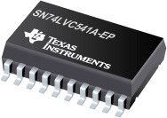
SN74LVC541A-EP 具有三态输出的增强型产品八路缓冲器/驱动器

The SN74LVC541A-EP octal buffer/driver is designed for 2.7-V to 3.6-V VCC operation.
The device is ideal for driving bus lines or buffering memory address registers.
This device features inputs and outputs on opposite sides of the package to facilitate printed circuit board layout.
The 3-state control gate is a 2-input AND gate with active-low inputs so that, if either output enable (OE1\ or OE2\) input is high, all eight outputs are in the high-impedance state.
Inputs can be driven from either 3.3-V or 5-V devices. This feature allows the use of this device as a translator in a mixed 3.3-V/5-V system environment.
This device is fully specified for partial-power-down applications using Ioff. The Ioff circuitry disables the outputs, preventing damaging current backflow through the device when it is powered down
| SN74LVC541A-EP | |
| Voltage Nodes (V) | 3.3, 2.7 |
| Vcc range (V) | 2.0 to 3.6 |
| Logic | True |
| Input Level | TTL/CMOS |
| Output Level | LVTTL |
| Output Drive (mA) | -24/24 |
| No. of Gates | |
| No. of Outputs | 8 |
| tpd max (ns) | 5.1 |
| Static Current | 0.01 |
| Rating | HiRel Enhanced Product |
| Technology Family | LVC |
SN74LVC541A-EP 特性
- Controlled Baseline
- One Assembly/Test Site, One Fabrication Site
- Extended Temperature Performance of –40°C to 125°C
- Enhanced Diminishing Manufacturing Sources (DMS) Support
- Enhanced Product-Change Notification
- Qualification Pedigree
- Operates From 2 V to 3.6 V
- Inputs Accept Voltages to 5.5 V
- Max tpd of 5.1 ns at 3.3 V
- Typical VOLP (Output Ground Bounce)
<0.8 V at VCC = 3.3 V, TA = 25°C - Typical VOHV (Output VOH Undershoot)
>2 V at VCC = 3.3 V, TA = 25°C - Supports Mixed-Mode Signal Operation on All Ports (5-V Input/Output Voltage With 3.3-V VCC)
- Ioff Supports Partial-Power-Down Mode Operation
SN74LVC541A-EP 芯片订购指南
| 器件 | 状态 | 温度 | 价格(美元) | 封装 | 引脚 | 封装数量 | 封装载体 | 丝印标记 |
| SN74LVC541AQDWREP | ACTIVE | -40 to 125 | 0.36 | 1ku | SOIC (DW) | 20 | 2000 | LARGE T&R | |
| SN74LVC541AQPWREP | ACTIVE | -40 to 125 | 0.36 | 1ku | TSSOP (PW) | 20 | 2000 | LARGE T&R | |
| V62/04666-01XE | ACTIVE | -40 to 125 | 0.36 | 1ku | SOIC (DW) | 20 | 2000 | LARGE T&R | |
| V62/04666-01YE | ACTIVE | -40 to 125 | 0.36 | 1ku | TSSOP (PW) | 20 | 2000 | LARGE T&R |
SN74LVC541A-EP 应用手册
SN74LVC541A-EP 质量与无铅数据
| 器件 | 环保计划* | 铅/焊球涂层 | MSL 等级/回流焊峰 | 环保信息与无铅 (Pb-free) | DPPM / MTBF / FIT 率 |
| SN74LVC541AQDWREP | Green (RoHS & no Sb/Br) | CU NIPDAU | Level-1-260C-UNLIM | SN74LVC541AQDWREP | SN74LVC541AQDWREP |
| SN74LVC541AQPWREP | Green (RoHS & no Sb/Br) | CU NIPDAU | Level-1-260C-UNLIM | SN74LVC541AQPWREP | SN74LVC541AQPWREP |
| V62/04666-01XE | Green (RoHS & no Sb/Br) | CU NIPDAU | Level-1-260C-UNLIM | V62/04666-01XE | V62/04666-01XE |
| V62/04666-01YE | Green (RoHS & no Sb/Br) | CU NIPDAU | Level-1-260C-UNLIM | V62/04666-01YE | V62/04666-01YE |
SN74LVC541A-EP 应用技术支持与电子电路设计开发资源下载
- SN74LVC541A-EP 数据资料 dataSheet 下载.PDF
- TI 德州仪器缓冲器、驱动器/收发器产品选型与价格 . xls
- (选择指南)逻辑器件指南 2009 (Rev. Z)
- (选择指南)小尺寸逻辑器件指南 (Rev. D)
- (用户指南)LOGIC Pocket Data Book
- (用户指南)Signal Switch Data Book
- (用户指南)LVC and LV Low-Voltage CMOS Logic Data Book
- (解决方案指南)2008年第一季度通信基础设施方案指南 (Rev. G)
- (解决方案指南)Communications Infrastructure Solutions Guide 1Q2010
