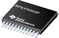
SN74LVTH543-EP 具有三态输出的增强型产品 3.3V Abt 八路寄存收发器

This octal transceiver is designed specifically for low-voltage (3.3-V) VCC operation, but with the capability to provide a TTL interface to a 5-V system environment.
The SN74LVTH543 contains two sets of D-type latches for temporary storage of data flowing in either direction. Separate latch-enable (LEAB\ or LEBA\) and output-enable (OEAB\ or OEBA\) inputs are provided for each register, to permit independent control in either direction of data flow.
The A-to-B enable (CEAB)\ input must be low to enter data from A or to output data from B. If CEAB is low and LEAB\ is low, the A-to-B latches are transparent; a subsequent low-to-high transition of LEAB\ puts the A latches in the storage mode. With CEAB\ and OEAB\ both low, the 3-state B outputs are active and reflect the data present at the output of the A latches
| SN74LVTH543-EP | |
| Voltage Nodes (V) | 3.3, 2.7 |
| Vcc range (V) | 2.7 to 3.6 |
| Input Level | TTL/CMOS |
| Output Level | LVTTL |
| Output Drive (mA) | -32/+64 |
| No. of Bits | 8 |
| Logic | True |
| Static Current | 5 |
| th (ns) | 1.6 |
| tpd max (ns) | 3.7 |
| tsu (ns) | 1 |
| Technology Family | LVT |
| Rating | HiRel Enhanced Product |
SN74LVTH543-EP 特性
- Controlled Baseline
- One Assembly/Test Site, One Fabrication Site
- Enhanced Diminishing Manufacturing Sources (DMS) Support
- Enhanced Product-Change Notification
- Qualification Pedigree
- Supports Mixed-Mode Signal Operation (5-V Input and Output Voltages With 3.3-V VCC)
- Typical VOLP (Output Ground Bounce)
<0.8 V at VCC = 3.3 V, TA = 25°C - Supports Unregulated Battery Operation Down to 2.7 V
- Ioff and Power-Up 3-State Support Hot Insertion
- Bus Hold on Data Inputs Eliminates the Need for External Pullup/Pulldown Resistors
- Latch-Up Performance Exceeds 500 mA Per JESD 17
- ESD Protection Exceeds JESD 22
- 2000-V Human-Body Model (A114-A)
- 200-V Machine Model (A115-A)
SN74LVTH543-EP 芯片订购指南
| 器件 | 状态 | 温度 | 价格(美元) | 封装 | 引脚 | 封装数量 | 封装载体 | 丝印标记 |
| SN74LVTH543IPWREP | ACTIVE | -40 to 85 | 1.05 | 1ku | TSSOP (PW) | 24 | 2000 | LARGE T&R | |
| V62/04677-01XE | ACTIVE | -40 to 85 | 1.05 | 1ku | TSSOP (PW) | 24 | 2000 | LARGE T&R |
SN74LVTH543-EP 应用手册
SN74LVTH543-EP 质量与无铅数据
| 器件 | 环保计划* | 铅/焊球涂层 | MSL 等级/回流焊峰 | 环保信息与无铅 (Pb-free) | DPPM / MTBF / FIT 率 |
| SN74LVTH543IPWREP | Green (RoHS & no Sb/Br) | CU NIPDAU | Level-1-260C-UNLIM | SN74LVTH543IPWREP | SN74LVTH543IPWREP |
| V62/04677-01XE | Green (RoHS & no Sb/Br) | CU NIPDAU | Level-1-260C-UNLIM | V62/04677-01XE | V62/04677-01XE |
SN74LVTH543-EP 应用技术支持与电子电路设计开发资源下载
- SN74LVTH543-EP 数据资料 dataSheet 下载.PDF
- TI 德州仪器缓冲器、驱动器/收发器产品选型与价格 . xls
- (选择指南)逻辑器件指南 2009 (Rev. Z)
- (选择指南)小尺寸逻辑器件指南 (Rev. D)
- (用户指南)LOGIC Pocket Data Book
- (用户指南)Signal Switch Data Book
- (用户指南)LVC and LV Low-Voltage CMOS Logic Data Book
- 2008年第一季度通信基础设施方案指南 (Rev. G)
- Communications Infrastructure Solutions Guide 1Q2010
- Design Summary for WCSP Little Logic
- Standard Linear & Logic for PCs, Servers & Motherboards
- STANDARD LINEAR AND LOGIC FOR DVD/VCD PLAYERS
- Military Low Voltage Solutions
- Low-Voltage Logic (LVC) Designer's Guide
- Logic Cross-Reference
