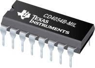
CD4054B-MIL CMOS 4 段液晶屏驱动器

CD4055B and CD4056B types are single-digit BCD-to-7-segment decoder/driver circuits that provide level-shifting functions on the chip. This feature permits the BCD input-signal swings (VDD to VSS) to be the same as or different from the 7-segment output-signal swings (VDD to VEE). For example, the BCD input-signal (VDD to VSS) may be as small as 0 to -3 V, whereas the output-display drive-signal swing (VDD to VEE) may be as large as from 0 to -15 V. If VDD to VEE exceeds 15 V, VDD to VSS should be at least 4V (0 to -4V). The 7-segment outputs are controlled by the DISPLAY-FREQUENCY (DF) input which causes the selected segment outputs to be low, high, or a square-wave output (for liquid-crystal displays). When the DF input is low the output segments will be high when selected by the BCD inputs.
|
CD4054B-MIL |
| Voltage Nodes (V) |
5, 10, 15 |
| Rating |
Military |
| Technology Family |
CD4000 |
CD4054B-MIL 特性
- Operation of liquid crystals with CMOS circuits provides ultra-low-power displays
- Equivalent ac output drive for liquid-crystal displays - no external capacitor required
- Voltage doubling across display, e.g. VDD - VEE = 18 V results in effective 36 V p-p drive across selected display segments
- Low- or high-output level dc drive for other types of displays
- On-chip logic-level conversion for different input- and output-level swings
- Full decoding of all input combinations: 0-9, L, H, P, A, -, and blank positions
- Strobed-latch function-CD4054B Series and CD4056B Series
- DISPLAY-FREQUENCY (DF) output for liquid-crystal common-line drive signal- CD4055B Series (CD4054B Series also: see introductory text)
- 100% tested for quiescent current at 20 V
- Maximum input current of 1 µA at 18 V over full package-temperature range; 100nA at 18 V and 25°C
- Noise margin (over full package-temperature range):
- 1 V at VDD = 5 V
- 2 V at VDD = 10 V
- 2.5 V at VDD = 15 V
- 5-V, 10-V, and 15-V parametric ratings
- Applications:
- General-purpose displays
- Calculators and meter
- Wall and table clocks
- Industrial control panels
CD4054B-MIL 芯片订购指南
| 器件 |
状态 |
温度 |
价格(美元) |
封装 | 引脚 |
封装数量 | 封装载体 |
丝印标记 |
| CD4054BF3A |
ACTIVE |
-55 to 125 |
5.91 | 1ku |
CDIP (J) | 16 |
1 | TUBE |
|
CD4054B-MIL 质量与无铅数据
| 器件 |
环保计划* |
铅/焊球涂层 |
MSL 等级/回流焊峰 |
环保信息与无铅 (Pb-free) |
DPPM / MTBF / FIT 率 |
| CD4054BF3A |
TBD |
A42 |
N/A for Pkg Type |
CD4054BF3A |
CD4054BF3A |
CD4054B-MIL 应用技术支持与电子电路设计开发资源下载
- CD4054B-MIL 数据资料 dataSheet 下载.PDF
- TI 德州仪器缓冲器、驱动器/收发器产品选型与价格 . xls
- CMOS 非缓冲反向器在振荡器电路中的使用 (PDF 951 KB)
- Semiconductor Packing Methodology (PDF 3005 KB)
- 逻辑产品选择指南 2006/2007 (修订版 Z)(4462KB)
- 标准线性和逻辑产品 5 分钟指南 (786KB)
- 了解和解释标准逻辑数据表
- LOGIC Pocket Data Book (PDF 6001 KB)
- HiRel Unitrode Power Management Brochure (PDF 206 KB)
- Logic Cross-Reference (PDF 2938 KB)

