HMC855LC5 28 Gbps 1:4 Demux SMT with Programmable Output Voltage
The HMC855LC5 is a 1:4 demultiplexer designed for data deserialization up to 28 Gbps. The device uses both rising and falling edges of the half-rate clock to sample the input data in sequence, D0-D3 and latches the data onto the differential outputs. A quarter-rate clock output generated on chip can be used to clock the data into other devices. The demux is DC coupled supporting broadband operation. All clock and data inputs to the HMC855LC5 are CML and terminated on-chip with 50 Ohms to the positive supply, GND, and may be DC or AC coupled. The differential outputs are source terminated to 50 Ohms and may also be AC or DC coupled. Outputs can be connected directly to a 50 Ohm ground terminated system, or drive devices with CML logic input. The HMC855LC5 also features an output level control pin, VR, which allows for loss compensation or signal level optimization. The HMC855LC5 operates from a single -3.3V supply and is available in RoHS compliant 5x5 mm SMT package.
技术特性
- Differential & Singe-Ended Operation
- Half Rate Clock Input
- Quarter Rate Reference Clock Output
- Fast Rise and Fall Times: 22 ps
- Low Power Consumption: 644 mW typ.
- Programmable Differential
Output Voltage Swing: 450 - 1144 mV
- Single Supply: -3.3V
- 32 Lead 5x5mm SMT Package: 25mm²
订购信息 Ordering Information
应用领域 APPLICATION
- SONET OC-192
- Broadband Test & Measurement
- Serial Data Transmission
up to 28 Gbps
- FPGA Interfacing
|
技术指标
Data/
Clock Rate (Gbps/GHz) |
Function |
Rise/Fall Time
(ps) |
Diff. Output Swing (Vp-p) |
DC Power Consumption (mW) |
DC Power Supply (Vdc) |
Package |
| 28 / 14 |
1:4 Demux with Adj. Vout |
22 / 22 |
0.45 - 1.14 |
644 |
-3.3 |
LC5 |
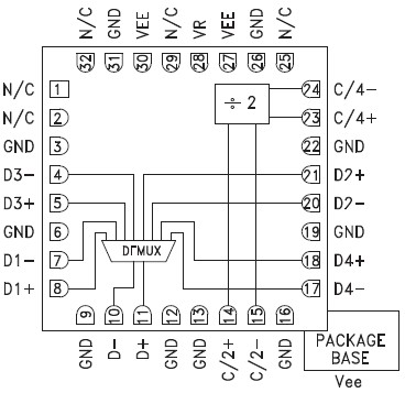
功能框图 Functional Block Diagram
|
